Semiconductor and semiconductor wafer fabrication requires an extremely high degree of precision and adherence to strict industry requirements. As such, it’s important that parts used in semiconductor manufacturing equipment exhibit exceptional quality and performance.
Since 1940, the experts at Hudson Technologies have offered superior quality metal stamping and deep drawn stamping services for our customers. We offer a full range of design, prototyping, production, and testing services to ensure that your custom semiconductor machinery components meet even the most rigorous specifications and requirements. Our state-of-the-art manufacturing facility is capable of producing custom semiconductor products for numerous applications, including:
- Filtering
- Pressure
- Vacuum
- Flow control
- Annealing
- Cryogenics
Components within Semiconductor Manufacturing Machinery
To function reliably, semiconductors must be manufactured with the utmost precision. This can be especially challenging in today’s market, where miniaturization is coupled with high-performance expectations. Using the latest deep drawn stamping technology, Hudson manufactures a variety of top-quality semiconductor manufacturing components, including:
Bellows
Bellows are precise, metal components that serve as a leak-tight seal and are designed to compress, bend, or extend to absorb angular or axial movement. These components are used in semiconductor fabrication machinery due to their ability to contain a vacuum, prevent contamination, and ensure an ultra-clean manufacturing environment. At Hudson Technologies, our deep drawn stamping capabilities allow us to create a range of conventional and welded-edge bellows, including:
- Pre-clean
- Orientor
- Load lock
- Slit
- Wafer lift
- Chamber lift
- Vacuum valve
Common applications for bellows in semiconductor fabrication machinery include:
- Slit valves
- Actuators
- Orientors
- Gas lines
- Connectors
- Gate valves
- Beam lines
- Motion feedthroughs
- Flexible couplings
- Lifters
- XYZ manipulators
- Leak detectors
- Valve stem seals
- Wafer handlers
- Torque couplings
- Ultra-high vacuum systems
MPS Sensors and Diaphragms
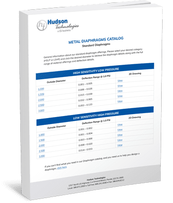
With decades of experience, Hudson is pleased to offer extensive metal diaphragm manufacturing services. Using the latest deep drawn stamping equipment, we can manufacture even the most complex metal diaphragms for your semiconductor manufacturing operation.
MPS sensors and diaphragms are used by semiconductor manufacturers to sense and transmit motion between steps in the fabrication process. As a stand-alone metal diaphragm manufacturer, we have extensive hands-on experience designing and creating reliable MPS sensors and pressure transducer diaphragms used in semiconductor manufacturing.
Unique Manufacturing Considerations for the Semiconductor Industry
Semiconductor manufacturing involves converting silicon and semiconductor metals from raw wafers into integrated circuits and other electronic components. There are many factors to consider throughout the manufacturing process to ensure optimal quality and performance.
For example, this process is usually performed in a clean room environment to avoid contamination and control conditions such as temperature, humidity, dust levels, and more. Another key consideration is the manufacturing machinery itself. Semiconductor manufacturing machinery is highly specialized and must be able to achieve very high tolerances on very small parts with no errors. Using top-quality machinery components guarantees the level of precision required by the semiconductor industry.
Common Manufacturing Methods Utilized
To create the highly accurate components necessary for quality semiconductor production, Hudson utilizes a variety of specialty stamping operations, including:
- Stage Tooling
- Progressive Die Tooling
- Metal-to-Rubber and Metal-to-Metal Tooling
- Transfer Tooling
When manufacturing custom semiconductor components, Hudson uses a unique combination of these processes. Our sizable facility holds more than 15,000 standard tooling products, and we are capable of creating custom tools to accommodate a variety of shape, size, and volume specifications within tight tolerances.
Industrial Machinery Components From Hudson Technologies
At Hudson Technologies, we are committed to producing precision machinery components for semiconductor manufacturing. We understand that semiconductor machinery components must perform with reliable, repeatable precision within exceptionally tight tolerances. No matter the size, shape, volume, or precision requirements for your semiconductor project, we have the knowledge, experience, and equipment to ensure optimal components.
Our team maintains regular communication with you throughout the process, from design and prototyping to production and testing. It is our goal to provide you with superior parts for all aspects of your semiconductor fabrication operation.
To learn more about our semiconductor component manufacturing capabilities and other deep drawn stamping services, contact our experts today or request a quote.
Producing Metal Parts For the Semiconductor Industry
Start With Silicon
All semiconductors rely on silicon to function properly. One of the most common elements on Earth, crude silicon appears in almost any variety of sand. However, suppliers must refine this silicon to nearly 100% purity if it is to function well in electronic applications.
Once it’s pure, workers heat the silicon to a molten state. This allows silicon to develop uniform chemical properties that make it ideal for later applications. After melting and reforming, workers lower a perfectly structured silicon “seed” into a larger vat of molten silicon. This seed creates the ideal conditions for long ingots of high-quality silicon to form.
Silicon’s ability to form long ingots of uniform material enable it to have the strong conductive capabilities that electronic applications rely on. What’s more, silicon is unique in that operators can modify when it can conduct electricity and when it can’t, hence the term “semiconductor.” This on/off capability forms the basis of binary code, i.e. the ones and zeros that dictate computer logic.
Using Photolithography to Pattern Silicon Chips
Manufacturers use photolithography to design the chips for their intended purpose. In this process, workers apply a pattern of photoresist across a wafer to create a “mask,” much like emulsion on film.
After this, workers etch away certain areas of the pattern. They do so by using plasma that degrades material with different properties than the hardened photoresist. Workers and automated processes repeat these steps, as well as deposition, diffusion, and ion implementation processes (outlined below), until they’ve created layers of transistors to their specifications.
Semiconductor manufacturers then use metallization to form interconnections between different transistors on the chip. This process also forms the chip’s bonding pads, which connect it to the package and the system’s circuit board.
Modifying the Semiconductor For Its Intended Use
Manufacturers perform a number of auxiliary tasks during photolithography to modify the semiconductor for its intended use. The most common processes include:
- Deposition: This process adds an insulating layer to the silicon substrate
- Diffusion: This process bakes impurities into wafer sections to alter their electrical characteristics
- Ion implantation: This process infuses silicon with various dopants to change its electrical characteristics
Where We Fit In
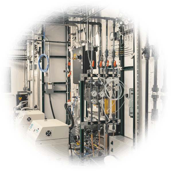
At Hudson Technologies, industry professionals come together to build essential components used to fabricate semiconductor wafers. We work with a wide range of materials, including:
- Titanium
- Stainless steel alloys
- Hastelloy
- Inconel
We also offer specialized tooling, finite element analysis (FEA) design, and customized packaging services depending on your needs. Hudson supplies much of the equipment found in fab plants, including machinery used for:
- Filtering
- Pressure
- Vacuum
- Flow control
- Annealing
- Cryogenics
The Hudson Difference
Hudson Technologies has led the way in designing industry-leading metal parts and diaphragms since our founding in 1940. We’re proud to be at the forefront of today’s custom metal stamping industry.
To learn more about our services and how they can help your applications, contact our team today.


